Welcome
de


AMD
XC6VLX365T-2FF1759I
FPGAs (Field Programmable Gate Array)
XC6VLX365T-2FF1759I
2-XC6VLX365T-2FF1759I

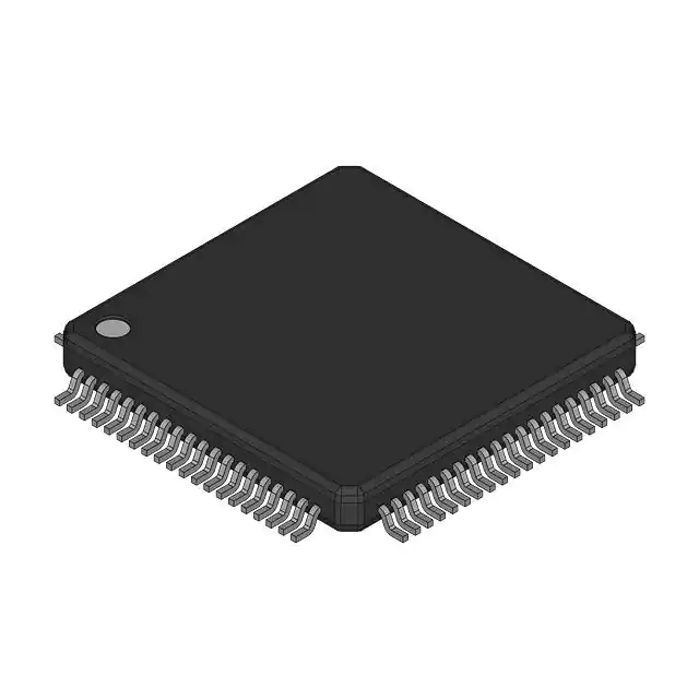
FPGA Virtex-6 LXT Family 364032 Cells 40nm Technology 1V 1759-Pin FCBGA
In Stock : Please Submit RFQ TO US
Not available
QUICK RFQ
ADD TO RFQ LIST
XC6VLX365T-2FF1759I Description
Tech Specifications
Min Operating Temperature
-40°C
Terminal Finish
Tin/Lead (Sn63Pb37)
Height Seated (Max)
3.5mm
Terminal Position
BOTTOM
Package / Case
FCBGA
Specifications
Value
Technology
CMOS
Terminal Form
BALL
Number of Pins
1759
Supply Voltage-Max (Vsup)
1.05V
Supply Voltage
1V
ECCN Code
3A001.A.7.A
Number of Logic Elements/Cells
364032
Qualification Status
Not Qualified
Pbfree Code
no
RoHS Status
RoHS Compliant
Moisture Sensitivity Level (MSL)
4
RAM Size
1.8MB
Number of Logic Blocks (LABs)
28440
Number of I/O
720
JESD-609 Code
e0
Number of Outputs
720
Time@Peak Reflow Temperature-Max (s)
NOT SPECIFIED
Max Operating Temperature
100°C
Peak Reflow Temperature (Cel)
NOT SPECIFIED
Programmable Logic Type
FIELD PROGRAMMABLE GATE ARRAY
Subcategory
Field Programmable Gate Arrays
Operating Supply Voltage
1V
Speed Grade
2
Terminal Pitch
1mm
Temperature Grade
INDUSTRIAL
XC6VLX365T-2FF1759I Documents
Download datasheets XC6VLX365T-2FF1759I
Related Parts
RTAX2000DL-1CQ352V
Actel
AGLN125V5-CSG81I
Microsemi
XCV200E-7BG256I
AMD
XC9572-3PQ100
AMD
QL8X12BL-2PL68C
QuickLogic
XCV1000E-8FG560C
AMD
XCV600-5BGG432I
AMD
XC5204-4VQ100I
AMD
XCR5064PC44-12I
AMD
AX1000-FGG676
Microsemi
XCR3064XL-VQ100C
AMD
A1280A-CQ172B
Actel
Shopping Guide
Payment Methods
Payment_desc
Shipping Rate
Shipping_rate_desc
Delivery Methods
Delivery_Methods_desc
Home_foot.INFORMATION
Home_foot.POLICIES
Home_foot.TOOLS
Home_foot.payment
Home_foot.Transportation
Home_foot.Trademark
Home_foot.Copyright